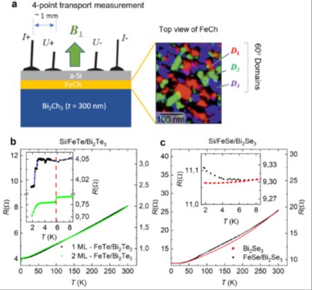
The phenomena at the interface of two different materials can differ significantly from the properties of the original materials. In our last work, we showed that a superconducting state is observed at the interface of a topological insulator Bi2Te3 with a thickness of 300 nm and a non-superconducting material FeTe with a thickness of one and two atomic layers. The opposite case is observed in a structure consisting of a topological insulator Bi2Se3 and a superconducting material FeSe, where superconductivity in FeSe is suppressed due to the presence of the interface of these two materials. In order to be able to use the FeTe/Bi2Te3 structure in practical applications, it is necessary to provide protection against the high reactivity of FeTe in air. For this reason, various protective layers on the FeTe surface were tested so as not to affect the superconducting state itself. Covering FeTe with amorphous silicon Si turned out to be a functional solution. The superconductivity of the resulting Si/FeTe/Bi2Te3 structure was characterized by measuring electrical transport. Structural analysis revealed that FeTe does not form a continuous layer on the surface of Bi2Te3 but islands of different sizes. Analysis of the transport properties showed that, depending on the size of the superconducting islands, we observe various types of superconducting states, which are characterized by different transition temperatures to the superconducting state.
The study was published in the prestigious journal nature partner journal 2d Materials and Applications [V. Tkáč et al., npj 2D Materials and Applications 8 (2024) 52] (https://doi.org/10.1038/s41699-024-00480-x), which has an impact factor of 9.2.