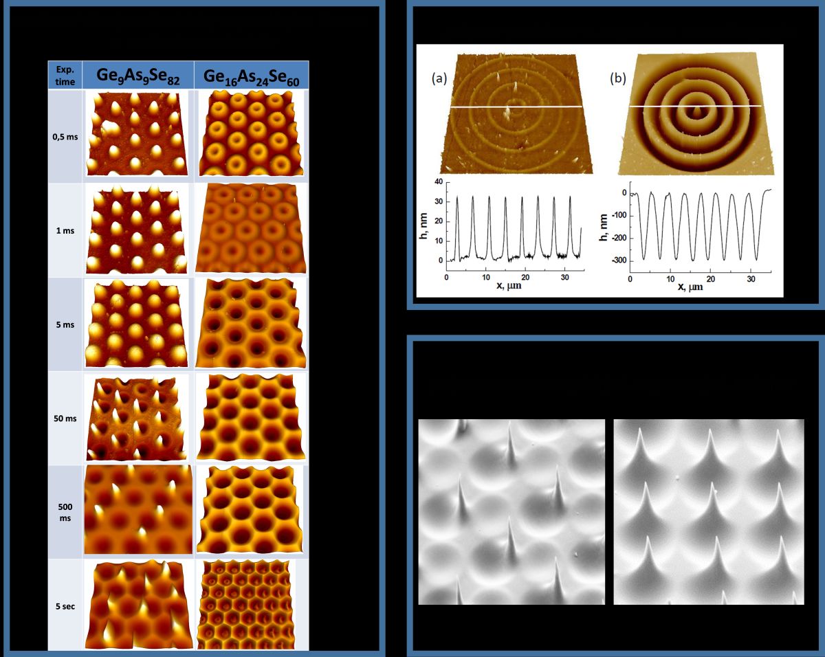
One of the new research directions conducted in our team in recent years was a study of interaction of a high-energy electron beam with thin layers of amorphous semiconductors. It has been found that these materials react sensitively to irradiation by the electrons and it is possible to create various structures on mesoscopic and nanoscopic scale. A unique result was the discovery of the formation of static Taylor cones, which have not yet been observed on the mesoscopic level. These discoveries have led to the development of new lithographic methods, interference hydrodynamic lithography as well as new possibilities for the direct preparation of positive and negative structures as well as structures with extremely high aspect ratio. Observed phenomena can be applied, for example, in the preparation of optical grids and waveguides, in the preparation of nano-emitters and probes for scanning probe microscopy [V. Kuzma, V. Bilanych, M. Kozejova, D. Hlozna, A. Feher, V. Rizak, V. Komanicky, Journal of Non-Crystalline Solids 456 7 (2017)].